Scratch & dig inspection
Introduction
Scratches and digs are surface impefections on optical elements, like lenses. Altough in general only 'cosmetic' in effect, it is important to identify and grade them in the manufacturing process. Even today, this inspection process is mostly based on visual inspection. Although human inspectors are flexibel, there are drawbacks concerning repeatability and reproducibility, and in terms of pace.
With respect to modern machine vision hardware and image processing capabilities, it is a valid question if such tasks could also be accomplished by an automatic inspection system (AIS). Present research in our group addresses the question to lay out such a system that would be capable to inspect an optical element with a single snapshot (without turning and tilting the element, as most inspectors usually do).
The first challenge is to choose the appropriate illumination, the imaging optics and -sensor. As benchmark, we pose the request to measure the size of 10µm large imperfections on an optical element with ~50mm diameter. It can be shown that is almost possible with state-of-the-art hardware.
Sensor resolution
As rough rule of thumb, on needs at least 2 pixels to resolve an object in an image. Consequently, for the 10µm scratch we need an sensor with about 10k x 10k pixels. This could be realized by scanning the optical element with a line scan camera - a valid approach, which will not be followed here. Instead, we prefer a matrix sensor, allowing to image the optical element with a single snap-shot. Such sensors are not yet available (at least not for civil use), but commercial sensors are already very close to this requirement.
Imaging optics
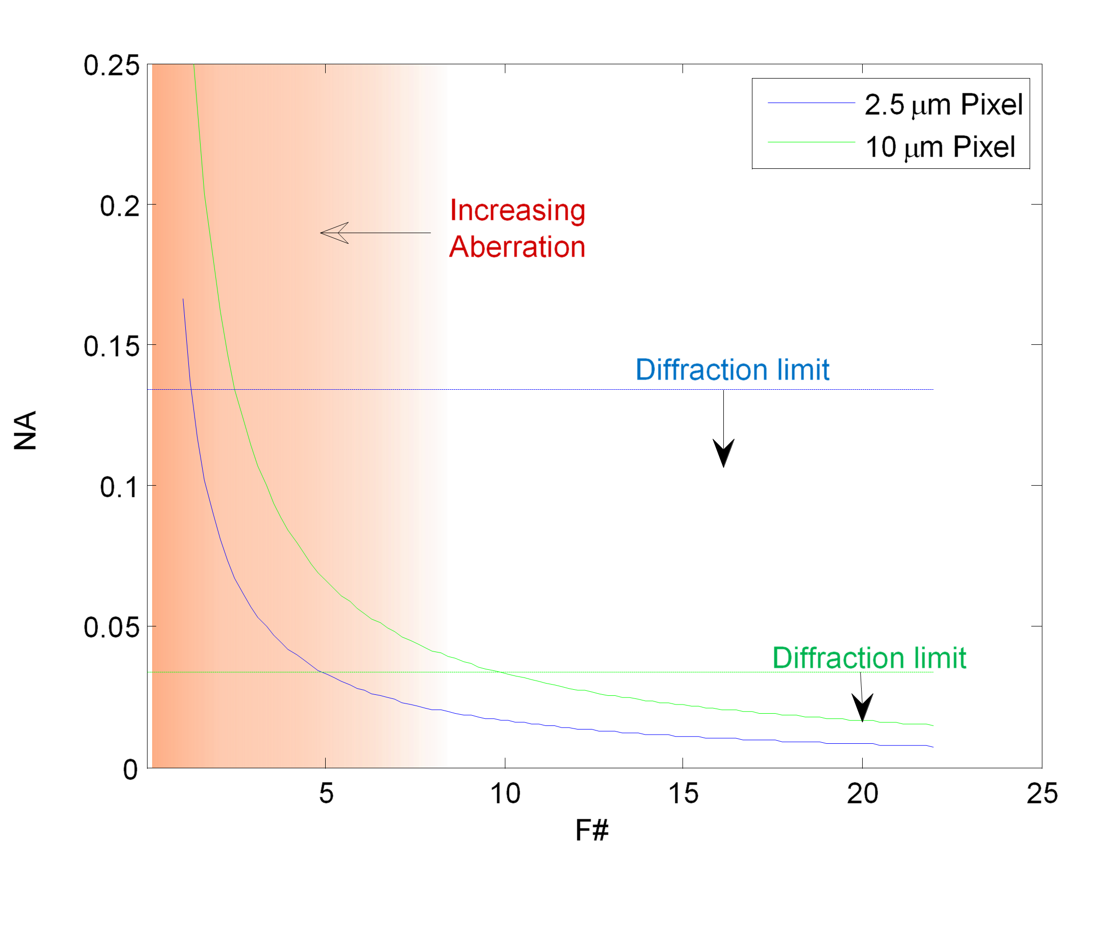
Imaging optics limits the system resolution by diffraction (determined by object side numerical aperture NA) and by lens aberrations (determined by F-number). Plotting these two design feature leads to the conclusion to choose a sensor with large pixels and a high quality lens, which allows an F-number in the range of <5 without detoriating resolution by aberation.
Besides, resolution is also limited by defocusing, a topic to be touched later.
Choice of illumination
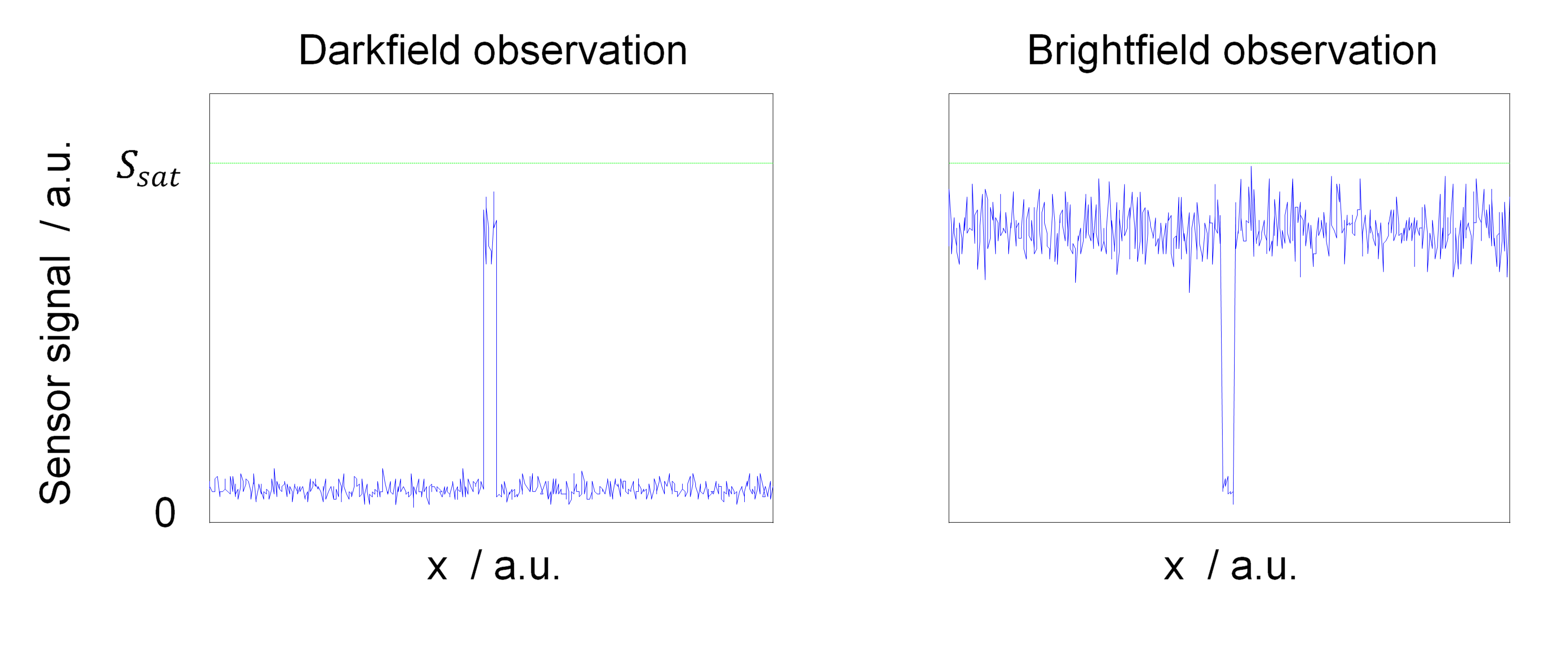
In brightfield conditions, the image of an imperfection appears dark on bright background, while under darkfield, the image is bright on a dark background.
The choice between brightfield and darkfield illumination can be taken on basis of a kind of Signal-to-Noise ratio, where the corresponding net sensor signal $S_{imp}$, as generated by an imperfection, is compared to the background noise $\sigma_{back}$
$ SBNR=\frac{| S_{imp}-S_{back} |}{\sigma_{back}}$.
It can be estimated that darkfield is about a factor of 10 better in $SBNR$ than brightfield. Brightfield also has the disadvantage to require a small F-number for the imaging optics. However, a darkfield configuration puts strict limits on the pose between illumination, optical element and imaging optics.
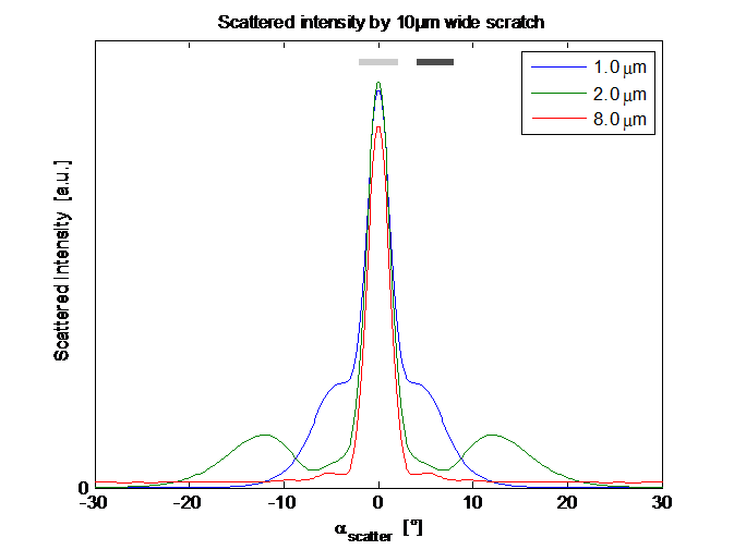
Scattering appears only in a small angle around the optical axis, as a simple simulation for a 10µm scratch shows (for different scratch depths). Gray bars on top of the curves indicate typical acceptance angles of brightfield and darkfield configurations.
Large imperfections cause an even smaller angular distribution.
Depth of Field
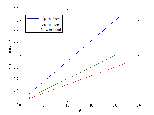
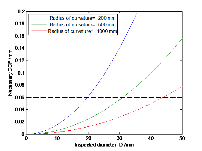
Small F-numbers, as required for high resolution, will cause small depth of field.
Consequently, only optical flats or lenses with large radii can be inspected with a single snap-shot.
There are several possibilities to achieve an extended depth of field. A straight foreward way is focus stacking, where the resulting image is composed of a stack of images. The example shown above is taken from a scratch reference target. The upper image shows the limited depth of field of a single image, the lower image is the result of focus stacking.